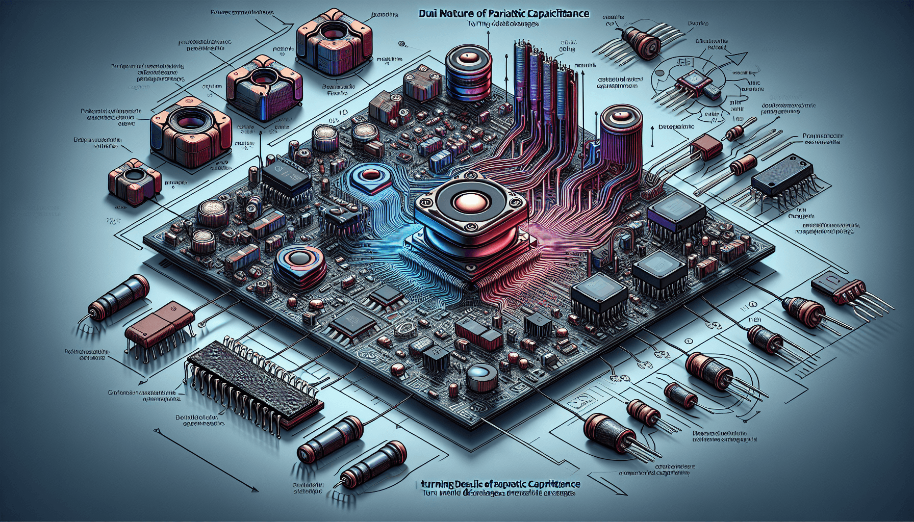
The Dual Nature of Parasitic Capacitance: Design Wisdom to Tackle EMC Challenges
Parasitic capacitance is often seen as an invisible enemy in electronic design, posing challenges to EMC performance. However, this article delves into the generation mechanisms, types of impacts, and solutions for parasitic capacitance from a professional perspective, proposing how to turn disadvantages into advantages by cleverly utilizing parasitic capacitance to enhance design efficiency and electromagnetic compatibility. It covers various application scenarios such as power semiconductors, magnetic devices, and PCB routing, supplemented with concrete cases and technical data, providing comprehensive practical references for electronic engineers.
Hal
post
0 /
Professional Insights: In-Depth Discussion on Parasitic Capacitance
This article provides a detailed introduction to the concept, impacts, and solutions of parasitic capacitance, serving as a valuable knowledge summary for engineers engaged in electronic design and electromagnetic compatibility (EMC) work. It not only describes the negative impacts of parasitic capacitance but also emphasizes its positive effects in specific contexts, presenting a convincing dialectical perspective.
The Dual Nature of Parasitic Capacitance: Crisis and Opportunity
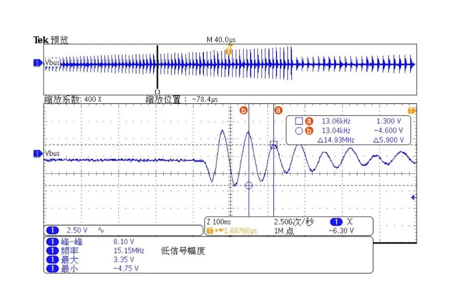
While parasitic capacitance is difficult to avoid, the author presents specific methods to “turn harm into benefit.” For instance, leveraging the characteristics of parasitic capacitance to resolve oscillation issues in switch-mode power supplies or appropriately adjusting power device parameters to optimize electromagnetic performance. This reminds us that what is often labeled as a “problem” in technical design may serve as a starting point for innovation.
In-Depth Technical Analysis: Detailed and Practical
The article thoroughly explains the generation mechanisms of parasitic capacitance in different scenarios, including:
- Parasitic capacitance in power semiconductors: such as CISS, COSS, CRSS in MOSFETs.
- Parasitic capacitance in magnetic devices: how inter-winding capacitance affects high-frequency noise.
- Parasitic capacitance in PCB routing: its correlation with crosstalk issues.
These specific cases and test data (e.g., EMI test results after replacing a MOSFET) not only add credibility but also provide practical references for engineers.
Comprehensiveness and Feasibility of Solutions
The author proposes a series of measures to address parasitic capacitance, ranging from device design, routing optimization to material selection. For example:
- Adding ferrite beads to suppress parasitic oscillation.
- Grounding heat sinks to reduce parasitic capacitance.
- Employing vertical crossing for PCB routing to minimize interference.
These methods consider theoretical aspects while ensuring practical operability, showcasing the author’s extensive practical experience.
Personal Insights and Questions
Potential Applications of Positive Effects The article mentions the reasonable utilization of parasitic capacitance to solve EMC problems. Could there be more specific discussions of successful practical cases? For instance, in which products has the clever use of parasitic capacitance reduced additional design costs or complexities?
Possibility of Dynamic Adjustments
Given that the parameters of parasitic capacitance can vary with device and structure changes, are there methods to dynamically adjust parasitic capacitance? For example, can certain structural parameters be actively controlled to adapt to different operating frequency requirements?
Integration with New Technologies
In high-speed signal transmission or 5G-related designs, does parasitic capacitance present new challenges or solutions? Especially concerning applications at ultra-high frequencies.
Conclusion
This article is both professional and in-depth, suitable for newcomers to grasp the basic concepts of parasitic capacitance, while also inspiring experienced engineers in tackling specific problems. Although parasitic capacitance is ubiquitous, its existence is not entirely negative; if utilized properly, it can become a hidden ally in design.
If you are interested in the article, I recommend reading the original text for more complete technical details and practical cases!
Keywords:
- Parasitic capacitance
- EMC performance optimization
- Power semiconductor design
- PCB routing techniques
- High-frequency noise suppression
- Electronic design practices
- EMI test improvement
- RC snubber circuits
- Distributed capacitance control
- Switch-mode power supply design


